AOI Inspection demystifiedAuthor : Adrian September 17,water-soluble solder paste 2025Table of ContentsIn the fast-paced world of printed circuit board (PCB) manufacturing, ensuring quality and precision is critical. One technology that stands out for achieving this is Automated Optical Inspection, commonly known as AOI. But what exactly is AOI inspection, and how does it impact the production process? In short, AOI is a non-contact, automated visual inspection method that uses cameras and advanced imaging to detect defects on PCBs, ensuring high-quality output. In this comprehensive guide, we’ll dive deep into the technology behind AOI, explore its key benefits and limitations, and explain why it’s a vital tool for modern electronics manufacturing. Whether you’re an engineer, a manufacturer, or simply curious about PCB production, this post will break down everything you need to know about AOI inspection.
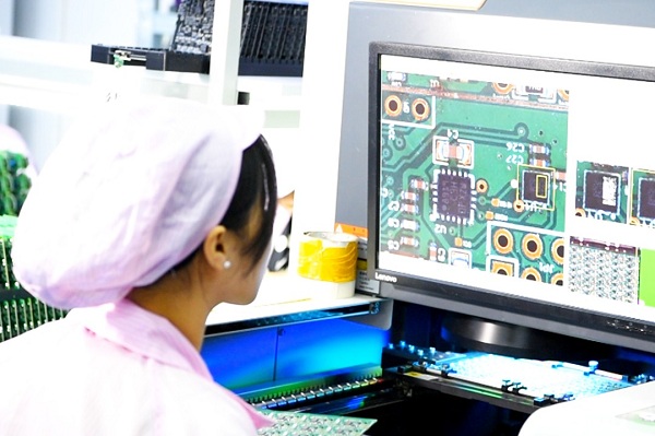
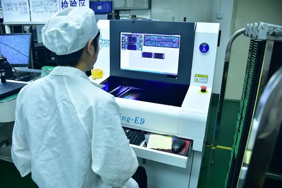
What Is AOI Inspection in PCB Manufacturing?Automated Optical Inspection (AOI) is a cutting-edge technology used in the manufacturing of printed circuit boards to identify defects and ensure quality. Unlike manual inspection methods, AOI relies on high-resolution cameras, sophisticated lighting systems, and advanced software algorithms to scan PCBs for issues. These systems can detect a wide range of problems, including missing components, solder defects, misaligned parts, and even surface imperfections, all without human intervention. AOI is typically integrated into various stages of the PCB production process, such as bare board inspection, solder paste inspection, pre-reflow, and post-reflow stages. By catching defects early, AOI helps manufacturers avoid costly rework and ensures that only high-quality boards move forward in the production line. This technology has become indispensable as PCBs grow more complex, with smaller components and tighter tolerances, such as 01005 components that measure just 0.4mm by 0.2mm.
How Does AOI Inspection Technology Work?The technology behind AOI inspection is a blend of hardware and software working together to achieve precise defect detection. Here’s a step-by-step breakdown of how it operates:
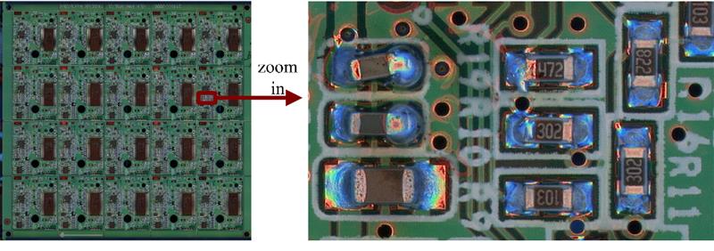
AOI systems are designed for sub-pixel accuracy, often achieving precision levels below 10 micrometers, which is crucial for inspecting modern miniaturized components. This level of detail ensures that even tiny deviations are caught before they become bigger problems.
The Pros of AOI Inspection in PCB ManufacturingAOI inspection offers numerous advantages that make it a cornerstone of modern PCB production. Below are some of the key benefits that manufacturers gain by implementing this technology. 1. High Accuracy and PrecisionWith the ability to detect defects at a sub-pixel level, AOI systems provide unmatched accuracy. For instance, they can identify misplacements as small as 0.05mm, which is critical for high-density boards with components packed tightly together. This precision reduces the risk of defective products reaching the market. 2. Speed and EfficiencyManual inspection of PCBs can take hours, especially for complex designs with thousands of components. AOI systems, on the other hand, can scan and analyze a board in seconds, inspecting up to 100 boards per hour in high-speed production lines. This speed boosts throughput and keeps production schedules on track. 3. Cost-Effectiveness in the Long RunWhile the initial investment in AOI equipment can be significant, the long-term savings are substantial. By catching defects early, AOI reduces the need for rework, which can cost manufacturers up to 30% more per board if issues are found later in the process. Additionally, it minimizes the risk of costly recalls or customer returns due to faulty products. 4. Versatility Across Production StagesAOI isn’t limited to one phase of manufacturing. It can be used for bare board inspection to check for scratches or shorts, during solder paste inspection to ensure even application (targeting 100% coverage), and post-reflow to verify component placement and soldering quality. This versatility makes it a valuable tool at multiple checkpoints. 5. Non-Contact InspectionUnlike some testing methods that require physical contact with the PCB, AOI is entirely non-contact. This eliminates the risk of damaging delicate components or solder joints during inspection, ensuring the board remains intact for further processing.
The Cons of AOI Inspection in PCB ManufacturingWhile AOI inspection brings significant benefits, it’s not without its challenges. Understanding these limitations can help manufacturers make informed decisions about integrating AOI into their processes. 1. High Initial InvestmentThe cost of acquiring and setting up an AOI system can be a barrier, especially for smaller manufacturers. Entry-level systems may start at tens of thousands of dollars, while high-end models with advanced features can exceed $100,000. This upfront cost may deter some businesses despite the long-term savings. 2. Limitations in Detecting Hidden DefectsAOI relies on visual inspection, which means it can only detect surface-level issues. Hidden defects, such as internal solder joint problems or issues beneath components in ball grid arrays (BGAs), are beyond its scope. For these, manufacturers often need to complement AOI with other methods like X-ray inspection. 3. Potential for False PositivesAOI systems can sometimes flag non-issues as defects, known as false positives. For example, a slight variation in solder shine due to lighting conditions might be mistaken for insufficient solder. These false calls can slow down production as operators must manually verify each flagged issue, potentially reducing efficiency by 10-15% in some setups. 4. Complexity in Setup and ProgrammingSetting up an AOI system requires technical expertise to program the software and define inspection parameters. If not configured correctly, the system may miss critical defects or generate excessive false alarms. This setup process can take days or weeks, depending on the complexity of the PCB designs being inspected. 5. Dependence on Lighting and Camera QualityThe effectiveness of AOI heavily relies on the quality of its lighting and camera systems. Poor lighting can obscure defects, while low-resolution cameras may fail to capture fine details on high-density boards. Upgrading these components to handle smaller components like 01005 packages can add to the overall cost.
Applications of AOI Inspection in PCB ManufacturingAOI inspection is a versatile tool that plays a critical role at various stages of PCB production. Here are some key applications where it delivers value:
By applying AOI at these stages, manufacturers can achieve a defect detection rate of over 95% in many cases, significantly improving product reliability.
Future Trends in AOI Inspection TechnologyAs PCB designs become more intricate, AOI technology continues to evolve to meet new challenges. Here are some trends shaping the future of AOI inspection:
How to Maximize the Benefits of AOI InspectionTo get the most out of AOI inspection, manufacturers should consider the following best practices:
Conclusion: Is AOI Inspection Right for Your PCB Manufacturing Process?Automated Optical Inspection (AOI) has transformed the way PCB manufacturers ensure quality and reliability in their products. With its high accuracy, speed, and versatility, AOI offers undeniable advantages, from catching defects as small as 0.05mm to inspecting hundreds of boards per hour. However, it’s not without challenges, including high initial costs and limitations in detecting hidden issues. By understanding both the pros and cons of AOI inspection technology, manufacturers can make informed decisions about integrating it into their production lines and pairing it with other methods for maximum effectiveness. As the electronics industry continues to push the boundaries of miniaturization and complexity, AOI will remain a vital tool, evolving with advancements like AI and 3D imaging to meet future demands. For any manufacturer aiming to deliver flawless PCBs, AOI inspection is not just an option—it’s a necessity for staying competitive in today’s market. Share · · · · The Role of Flux in PCB Wave Soldering: Selection, Application, and Residue RemovalMarch 16, 2026PCB wave soldering flux types include rosin, water-soluble, and no-clean options with varying activity levels for oxide removal and solder flow. This guide covers selection criteria, spray foam drop-jet application methods, residue removal processes, and alternatives like nitrogen blanketing to boost joint reliability and yields for engineers. Article Achieving Uniform Solder Fillets in PCB Wave Soldering: Process ControlMarch 16, 2026Achieve uniform solder fillets in PCB wave soldering with process control strategies. Optimize flux, preheat, wave height, conveyor speed for consistent fillet shape, height, and wetting balance. Includes visual inspection tips and troubleshooting for reliable through-hole assemblies. Boost quality in production. Article Optimizing Conveyor Speed for Efficient PCB Wave SolderingMarch 16, 2026Learn PCB wave soldering conveyor speed calculation to manage dwell time, immersion depth, and throughput effectively. Electric engineers get practical steps, best practices, and troubleshooting tips for higher process efficiency and fewer defects in wave soldering operations. Article Understanding IPC Standards for PCB Surface Finishes: Ensuring Quality and ComplianceMarch 11, 2026Understand IPC standards IPC 4552 ENIG and IPC 4553 immersion silver for PCB surface finishes. Ensure compliance, enhance solderability, and prevent common defects to achieve reliable, high quality circuit boards. Article Miniaturization Challenges in PCB AssemblyMarch 11, 2026Navigate the complexities of high density interconnect PCB assembly and precise component placement. Learn to tackle miniaturization challenges, from tiny part handling to thermal stress, ensuring robust and reliable electronics. Article High Speed Routing Techniques: PCBMarch 11, 2026Master high speed routing in PCBs to ensure signal integrity and minimize electromagnetic interference. Learn essential techniques for robust designs, from controlled impedance to differential pair strategies. Prevent performance issues and achieve reliable electronics. ArticleGet Instant PCB |